- 您现在的位置:买卖IC网 > Sheet目录3861 > PIC18F45K80-I/ML (Microchip Technology)MCU PIC 32KB FLASH 44QFN
PIC18F66K80 FAMILY
DS39977F-page 128
2010-2012 Microchip Technology Inc.
6.6.3
MAPPING THE ACCESS BANK IN
INDEXED LITERAL OFFSET MODE
The use of Indexed Literal Offset Addressing mode
effectively changes how the lower part of Access RAM
(00h to 5Fh) is mapped. Rather than containing just the
contents of the bottom part of Bank 0, this mode maps
the contents from Bank 0 and a user-defined “window”
that can be located anywhere in the data memory
space.
The value of FSR2 establishes the lower boundary of
the addresses mapped into the window, while the
upper boundary is defined by FSR2 plus 95 (5Fh).
Addresses in the Access RAM above 5Fh are mapped
as previously described. (See Section 6.3.2 “Access
.) An example of Access Bank remapping in this
addressing mode is shown in Figure 6-10.
Remapping the Access Bank applies only to operations
using the Indexed Literal Offset mode. Operations that
use the BSR (Access RAM bit = 1) will continue to use
Direct Addressing as before. Any Indirect or Indexed
Addressing operation that explicitly uses any of the
indirect file operands (including FSR2) will continue to
operate as standard Indirect Addressing. Any instruc-
tion that uses the Access Bank, but includes a register
address of greater than 05Fh, will use Direct
Addressing and the normal Access Bank map.
6.6.4
BSR IN INDEXED LITERAL
OFFSET MODE
Although the Access Bank is remapped when the
extended instruction set is enabled, the operation of the
BSR remains unchanged. Direct Addressing, using the
BSR to select the data memory bank, operates in the
same manner as previously described.
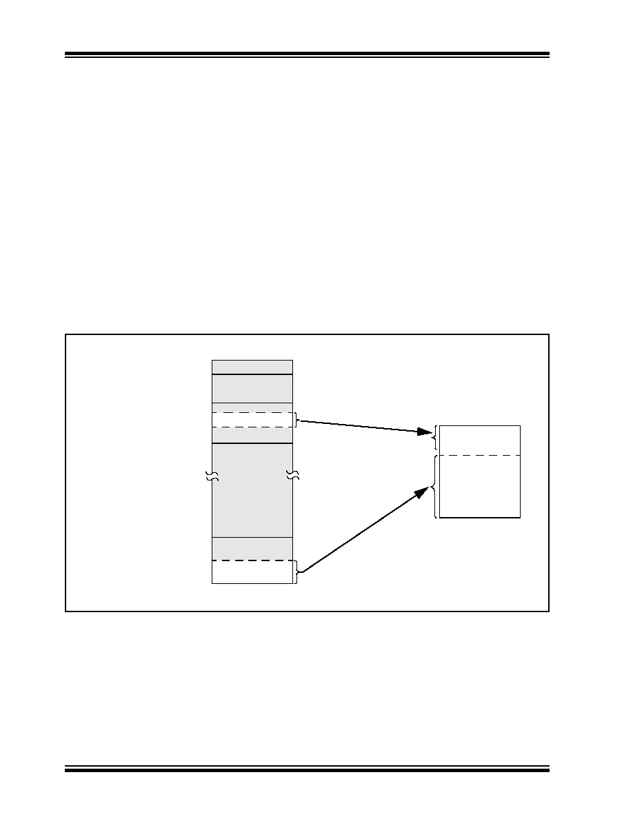
FIGURE 6-10:
REMAPPING THE ACCESS BANK WITH INDEXED LITERAL
OFFSET ADDRESSING
Data Memory
000h
100h
200h
F60h
F00h
FFFh
Bank 1
Bank 15
Bank 2
through
Bank 14
SFRs
05Fh
ADDWF f, d, a
FSR2H:FSR2L = 120h
Locations in the region
from the FSR2 Pointer
(120h) to the pointer plus
05Fh (17Fh) are mapped
to the bottom of the
Access RAM (000h-05Fh).
Special Function Registers
at F60h through FFFh are
mapped to 60h through
FFh, as usual.
Bank 0 addresses below
5Fh are not available in
this mode. They can still
be addressed by using the
BSR.
Access Bank
00h
FFh
Bank 0
SFRs
Bank 1 “Window”
Not Accessible
Window
Example Situation:
120h
17Fh
5Fh
60h
发布紧急采购,3分钟左右您将得到回复。
相关PDF资料
PIC24F32KA302-I/ML
MCU 32KB FLASH 2KB RAM 28-QFN
PIC18LF45K80-I/ML
MCU PIC ECAN 32KBFLASH 44QFN
PIC18F4221-I/PT
IC PIC MCU FLASH 2KX16 44TQFP
PIC18F1320-I/SO
IC MCU FLASH 4KX16 A/D 18SOIC
PIC18LF2321-I/SS
IC PIC MCU FLASH 4KX16 28SSOP
PIC16F917-I/PT
IC PIC MCU FLASH 8KX14 44TQFP
PIC18F1320-I/SS
IC MCU FLASH 4KX16 A/D 20SSOP
PIC24FV32KA301-I/P
MCU 32KB FLASH 2KB RAM 20-PDIP
相关代理商/技术参数
PIC18F45K80-I/P
功能描述:8位微控制器 -MCU 32KB FL 4KBRM 16MIPS 12bit ADC CTMU RoHS:否 制造商:Silicon Labs 核心:8051 处理器系列:C8051F39x 数据总线宽度:8 bit 最大时钟频率:50 MHz 程序存储器大小:16 KB 数据 RAM 大小:1 KB 片上 ADC:Yes 工作电源电压:1.8 V to 3.6 V 工作温度范围:- 40 C to + 105 C 封装 / 箱体:QFN-20 安装风格:SMD/SMT
PIC18F45K80-I/PT
功能描述:8位微控制器 -MCU 32KB FL 4KBRM 16MIPS 12bit ADC CTMU RoHS:否 制造商:Silicon Labs 核心:8051 处理器系列:C8051F39x 数据总线宽度:8 bit 最大时钟频率:50 MHz 程序存储器大小:16 KB 数据 RAM 大小:1 KB 片上 ADC:Yes 工作电源电压:1.8 V to 3.6 V 工作温度范围:- 40 C to + 105 C 封装 / 箱体:QFN-20 安装风格:SMD/SMT
PIC18F45K80T-I/ML
功能描述:8位微控制器 -MCU 32KB FL 4KBRM 16MIPS 12bit ADC CTMU RoHS:否 制造商:Silicon Labs 核心:8051 处理器系列:C8051F39x 数据总线宽度:8 bit 最大时钟频率:50 MHz 程序存储器大小:16 KB 数据 RAM 大小:1 KB 片上 ADC:Yes 工作电源电压:1.8 V to 3.6 V 工作温度范围:- 40 C to + 105 C 封装 / 箱体:QFN-20 安装风格:SMD/SMT
PIC18F45K80T-I/PT
功能描述:8位微控制器 -MCU 32KB FL 4KBRM 16MIPS 12bit ADC CTMU RoHS:否 制造商:Silicon Labs 核心:8051 处理器系列:C8051F39x 数据总线宽度:8 bit 最大时钟频率:50 MHz 程序存储器大小:16 KB 数据 RAM 大小:1 KB 片上 ADC:Yes 工作电源电压:1.8 V to 3.6 V 工作温度范围:- 40 C to + 105 C 封装 / 箱体:QFN-20 安装风格:SMD/SMT
PIC18F4610-E/ML
功能描述:8位微控制器 -MCU 64KB 3968 RAM 36 I/O RoHS:否 制造商:Silicon Labs 核心:8051 处理器系列:C8051F39x 数据总线宽度:8 bit 最大时钟频率:50 MHz 程序存储器大小:16 KB 数据 RAM 大小:1 KB 片上 ADC:Yes 工作电源电压:1.8 V to 3.6 V 工作温度范围:- 40 C to + 105 C 封装 / 箱体:QFN-20 安装风格:SMD/SMT
PIC18F4610-E/P
功能描述:8位微控制器 -MCU 64KB 3968 RAM 36 I/O RoHS:否 制造商:Silicon Labs 核心:8051 处理器系列:C8051F39x 数据总线宽度:8 bit 最大时钟频率:50 MHz 程序存储器大小:16 KB 数据 RAM 大小:1 KB 片上 ADC:Yes 工作电源电压:1.8 V to 3.6 V 工作温度范围:- 40 C to + 105 C 封装 / 箱体:QFN-20 安装风格:SMD/SMT
PIC18F4610-E/PT
功能描述:8位微控制器 -MCU 64KB 3968 RAM 36 I/O RoHS:否 制造商:Silicon Labs 核心:8051 处理器系列:C8051F39x 数据总线宽度:8 bit 最大时钟频率:50 MHz 程序存储器大小:16 KB 数据 RAM 大小:1 KB 片上 ADC:Yes 工作电源电压:1.8 V to 3.6 V 工作温度范围:- 40 C to + 105 C 封装 / 箱体:QFN-20 安装风格:SMD/SMT
PIC18F4610-I/ML
功能描述:8位微控制器 -MCU 64KB 3968 RAM 36 I/O RoHS:否 制造商:Silicon Labs 核心:8051 处理器系列:C8051F39x 数据总线宽度:8 bit 最大时钟频率:50 MHz 程序存储器大小:16 KB 数据 RAM 大小:1 KB 片上 ADC:Yes 工作电源电压:1.8 V to 3.6 V 工作温度范围:- 40 C to + 105 C 封装 / 箱体:QFN-20 安装风格:SMD/SMT